|
埃德万斯采访新闻稿-20161027非硅微纳机电制造领域的工匠精神——埃德万斯盛大亮相纳博会
2016年10月26日,由中华人民共和国科学技术部、中国科学院、江苏省人民政府、中国科学院上海微系统与信息技术研究所传感技术联合国家重点实验室主办的,由上海龙媒商务咨询有限公司、江苏省纳米技术创新中心承办的“2016传感器与MEMS技术产业化国际研讨会暨科研成果产品展”与“中国国际纳米技术产业博览会(CHInano2016 Conference& Expo)”在苏州国际博览中心同期联合举办。
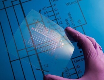
北京埃德万斯离子束技术研究所有限公司(以下简称:埃德万斯)首次在纳博会上盛大亮相,并全面展示了由其自主研发的设备制成的各类样品,包括蓝宝石基底Si膜、Ti膜、Pt膜及10μm厚铝膜;应用于高频宽带光学通信的AlN膜;应用于可穿戴设备、柔性集成电路的柔性材料镀金属薄膜;应用于高端新型电子元器件的合金薄膜电阻;应用于航天、导弹、新型雷达的高温超导射频器件;以及微机械器件等。
利用埃德万斯自主研发的设备制成的微结构
可弯折柔性集成电路 埃德万斯是国内著名的先进商用离子束技术产品专业制造者,前身为在钱学森提议下成立的航天二院23所“离子束技术、工艺及成套设备系统工程部”。公司创始人为国际知名离子束技术专家刘金声研究员,从上世纪八十年代起,刘金声老师历经38年潜心钻研离子束技术,率先在国内成功研发出离子束技术应用成套设备,成为了国内这一行业的领跑者,为埃德万斯今日的腾飞打下坚实的基础。 埃德万斯多年来一直服务于国内航天、军工两大领域,提供工艺技术和配套设备,为国家重大型号任务做出卓著贡献,如:卫星多轨扫描高分辨率红外探测器;军用的红外成像系统;提供精密惯性制导陀螺生产线,研制光纤陀螺和卫星晶振系统专用离子束系统等。随着综合服务能力的提升,逐渐将服务扩大到中科院、清华、北大等顶尖级的国内科研院校,以及美国麻省理工大学、沙特阿卜杜拉国王科技大学等国外名校。起始至今离子束技术应用设备累计提供了200多台。
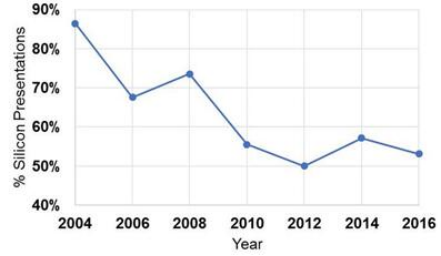
同时,在本次国际研讨会上,埃德万斯发言人殷睿婷女士还发表了题为“Application of Ion Beam in Non-silicon MEMS”(离子束技术在非硅MEMS中的应用)的英文演讲。演讲中提到,随着应用场景的复杂化、终端产品的多样化,硅MEMS传感器应用范围越来越受局限,众多国际知名厂商开始注重新材料、新工艺、新技术的开发,国内外MEMS呈现从“硅”到“非硅”的发展趋势。 据麦姆斯咨询报道,在近些年的“固态传感器、执行器及微系统研讨会”上(The Solid State Sensors, Actuators and Microsystems Workshop,是最高水平MEMS新技术的展示舞台,该国际研讨会是MEMS领域最具竞争力的会议之一),出现了令硅材料从业者感到不安的趋势——关于硅材料技术的论文数量逐年降低。在2016年6月的研讨会上,仅有53%的演讲论文是关于硅材料器件的(只要器件中包含了硅材料,无论是作为被动基底还是活性材料)。
固态传感器、执行器及微系统研讨会中硅基器件演讲论文的比例 从过去12年来的演讲主题可以清晰的看出,硅材料微型器件的学术研究热潮已经开始逐渐消退。学术研究人员现在开始专注于开发聚合物和纸基微型器件。利用这些材料开发的器件,不仅工艺环保,而且制作设备简单、成本较低。相对硅材料,它们大幅缩减了研发经费预算。许多聚合物和纸基微型器件的创新都指向了医疗应用,对该领域来说,生物相容性和材料的柔性是基本要求。 面对这一产业发展趋势,埃德万斯自主研发的离子束技术应用设备迎来春天。埃德万斯第四代离子束技术应用系统可加工材料范围广泛,可用于刻蚀加工各种金属、合金、非金属、氧化物、氮化物、碳化物、半导体、聚合物、陶瓷、红外、超导甚至生物组织等各种材料。 埃德万斯现已初步搭建成“自主设备开发+工艺技术研发+项目加速孵化+代工生产基地”的全产业链生态布局。与国内知名加速器企业砹立方合作运营的,由国富资本等多支产业基金对接支持的埃德万斯微纳制造产业加速孵化器即将揭牌。该垂直产业加速孵化器具有高度专注、重度垂直的特点,政府融资加外界资本的介入,将助推企业快速成长。埃德万斯还计划在深圳建设代加工生产基。埃德万斯将一如既往潜心打造设备,加大工艺研发力度,用好产业资本快速孵化,筑造专业代工基地,为我国产业的提升及转型贡献力量。
Non Silicon Micro Nano Electromechanical Manufacturing Craftsman Spirit -- ADVANCED Grand Debut Nabo Conference In October 26, 2016, sponsored by the People's Republic of China science and technology research department, China Academy of Sciences, Jiangsu Provincial People's government, Chinese Shanghai Institute of micro system and information technology statekeylaboratoriesoftransducertechnology, hosted by Shanghai dragon Media Business Consulting Co., Ltd. and Jiangsu province nanotechnology innovation center "2016 sensor and MEMS technology industrialization international Symposium scientific research and product exhibition" and "China international nanotechnology industry expo (CHInano2016 Conference& Expo)" held in Suzhou International Expo Center during the same period. Beijing advanced ion beam Technology Research Institute Co. Ltd. (hereinafter referred to as: Advanced) debut in nabok grand meeting, and fully demonstrated the made its self-developed equipment all kinds of samples, including sapphire substrate Si film, Ti film, Pt film and 10 m thick aluminum film; AlN film used in high frequency broadband optical communication; flexible materials used in wearable devices, flexible integrated circuit of the metal plating film; alloy thin film resistor used in high-end new electronic components; High Temperature Superconducting RF devices used in aerospace, missile and radar model; and micro mechanical devices etc.. The use of micro structure made of advanced self-developed equipment Flexible flexible integrated circuit Ed Vance is the famous domestic advanced commercial ion beam technology products manufacturer, formerly known as Tsien Hsueshen proposed the establishment of second academy 23 "ion beam technology, technology and equipment system engineering department". Company founder of international famous ion beam technology expert Liu Jinsheng researcher, from late 80s onwards, Liu Jinsheng teacher after 38 years of painstaking study of ion beam technology, the first in China successfully developed the application of ion beam technology and equipment, has become the domestic industry leader, a solid foundation for the development of today's advanced. Advanced years of service in the domestic space, two military areas, to provide technology and equipment, to make outstanding contributions, for major national type tasks such as satellite multitrack scanning high resolution infrared detector; infrared imaging system protection; to provide precision inertial guidance gyroscope production line, development of special ion optical fiber gyro and satellite oscillator system beam system. With the comprehensive service capabilities, service will gradually expand to the Chinese Academy of Sciences, Tsinghua University, Beijing University and other top domestic research institutions, and MIT, Saudi King Abdullah University of science and technology and other foreign schools. Since the beginning, the ion beam technology application equipment has accumulated more than 200 units. At the same time, the International Symposium on advanced spokesman Ms. Yin Ruiting also published an article entitled "Application of Ion Beam in Non-silicon MEMS" (the application of ion beam technology in non silicon MEMS in the English speech). Mentioned in the speech, with diverse and complex, the terminal product application scenarios, the application range of silicon MEMS sensor is more and more limited, many international well-known manufacturers began to develop new material and technology, focusing on the domestic and foreign MEMS present from "Si" to "non silicon" trend of development. According to Mr James consultation reports, in recent years the "solid state sensors, actuators and Microsystems forum" (The Solid State Sensors Actuators and, Microsystems Workshop, is a new technology which is the highest level MEMS stage show, the International Symposium on the field of MEMS is one of the most competitive Conference), appeared to practitioners of silicon materials feel uneasy about the trend: the quantity of silicon material and technology papers decreased year by year. In the June 2016 workshop, only 53% of the speech papers were on silicon material devices (as long as the devices contained silicon material, either as passive substrate or as active material). Solid state sensors, actuators and Microsystems symposium, silicon devices, lecture papers, percentage It is clear from the topic of speech over the past 12 years that the academic research craze for silicon materials micro devices has begun to fade. Academic researchers are now focusing on developing polymers and paper based microdevices. The devices developed with these materials are not only environmentally friendly, but also easy to manufacture and low in cost. Relative to silicon materials, they substantially reduce R & D budget. Many innovations in polymers and paper based devices point to medical applications, and biocompatibility and material flexibility are essential requirements for the field. In the face of this industry development trend, independent research and development of advanced applications of ion beam technology equipment to usher in the spring. The four generation Aidewansidi ion beam technology application system can process a wide range of materials, can be used for etching processing all kinds of metal, alloy, metal, oxides, nitrides, carbides, semiconductors, polymers, ceramics, infrared, superconducting and biological tissue and other materials. Advanced has been initially built into the whole industry chain of ecological layout independent equipment development + technology + R & D project to accelerate the incubation + OEM production base ". With the cooperative operation of domestic well-known cubic astatine accelerator enterprises, backed by the wealth capital and many other branches of industry fund docking Ed million Siwei nano manufacturing industry to accelerate the incubators will be inaugurated. The vertical industry to accelerate the incubator has a high degree of attention, serious vertical features, government financing and external capital involvement, will boost the rapid growth of enterprises. Ed Vance also plans to build a production base in Shenzhen. As in the past will strive to build the equipment advanced technology research and development, increase efforts to make good use of industrial capital fast hatching, build professional OEM base for China's industrial upgrading and transformation of contribution. |


